Programmable Logic Devices I Have Used
(Click on each thumbnail image for a larger version.)
Introduction
Over the past 40+ years I have designed several projects that used programmable logic in order to reduce the number of ICs required on a board.
This web page only describes those of my projects that were actually built (even if not completely finished). However, over the years I also started designing various other projects that incorporated programmable logic, which were never (or at least not yet) built.
PAL16R8A and PAL16L8A
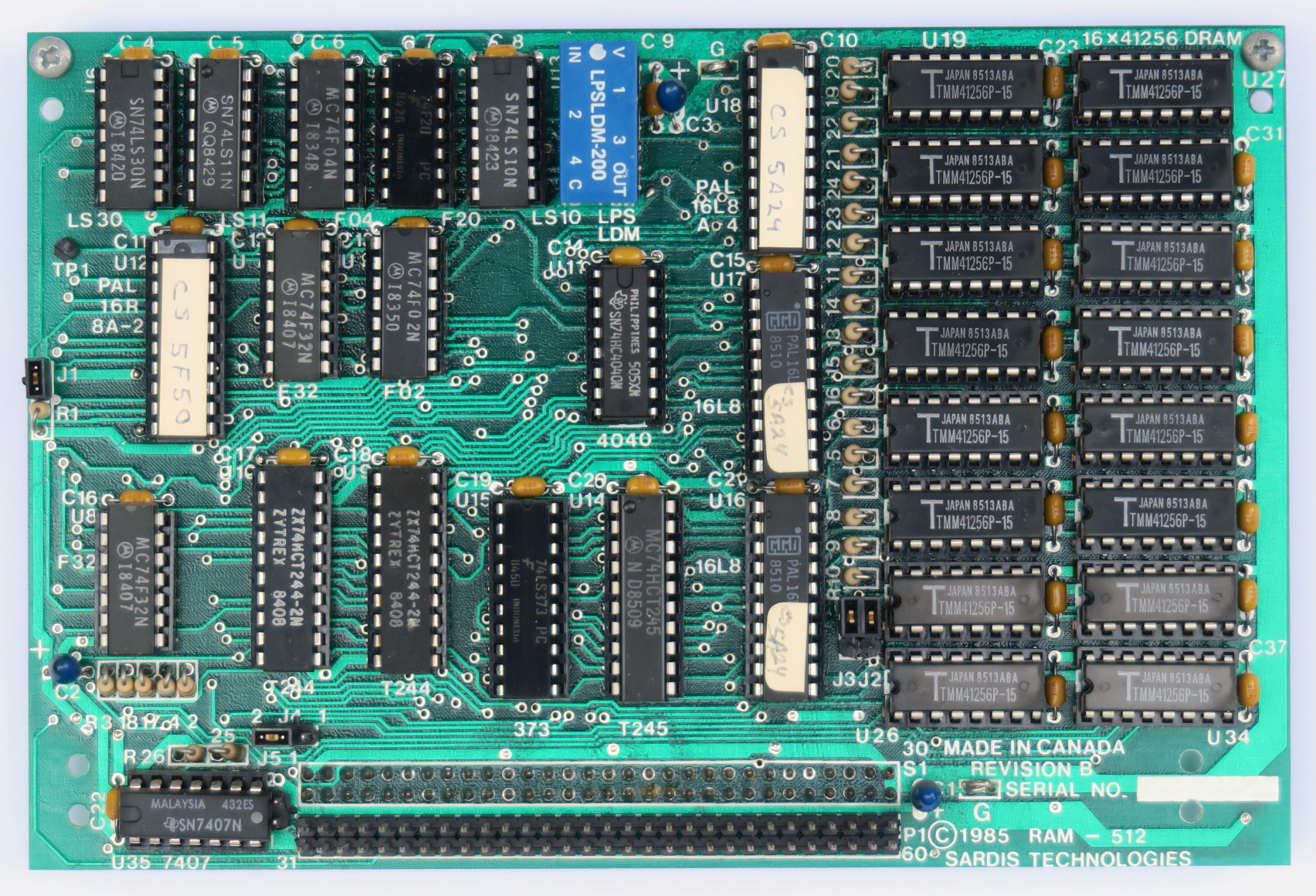
The RAM-512 board for the ST-2900, designed and built in 1985, uses one PAL16R8A-2 and three identically programmed PAL16L8A-4 chips. The logic equations are shown in the RAM-512 user manual, and you can find the device datasheet for them here. These were the very first programmable logic chips that I used in any of my projects.
Each PAL16L8A-4 chip implements a 3-channel multiplexer, with each channel having 3 inputs and 2 simultaneous outputs. The outputs connect to the address lines of the even and odd DRAM banks, allowing one bank to be refreshed in the same bus cycle as the other bank has data read from or written to it. Implementing this logic with standard 74LSxx parts would have required too many chips, so would not have fit into the desired board size, and the propagation delays would have been too great.
I used PALASM running on a borrowed IBM PC compatible computer (since I didn't yet own one) to design the logic for these PAL chips, and had them programmed by the distributor, who was R.A.E. Industrial Electronics (see History section) in Burnaby BC Canada.
PAL20L10

In 1986 I started designing a new floppy disk controller cartridge for the Radio Shack Color Computer (CoCo). The DMC ("No Halt" Dual Mode Controller), and its later PAL-4 daughterboard, use a 24-pin PAL20L10 (1.44MB .pdf) chip in order to reduce the number of ICs so they would all fit onto a standard CoCo cartridge size board.
However, this bipolar PAL is very power hungry, which is a major reason why my cartridge draws more current than the CoCo's power supply is supposed to deliver to its expansion slot.
I again used PALASM to design the logic for this PAL chip.
Lattice ispLSI 1032 and 1016
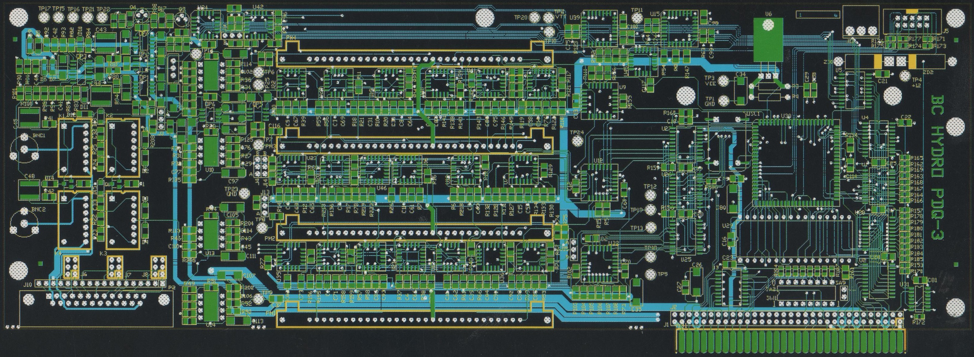
Probably in 1992 or 1993, while I was working for BC Hydro, one of the engineers in my department designed a sophisticated system to measure partial discharge in hydroelectric generator windings. Besides using some very fast ECL comparators and logic chips, he also used many 74HCxx chips in his board design. By this time I was aware of the new Lattice ispLSI 1032 (622KB .pdf) CMOS CPLD that was electrically erasable and in-system programmable. I convinced them that I could replace over two dozen 74HCxx chips with one 84-pin CPLD, greatly simplifying the board and its layout, as well as converting most of the asynchronous logic into synchronous logic. They then gave me the task to design the logic equations for this chip.
Lattice supplied easy-to-use design software (called pDS) that ran under Microsoft Windows, except that moving equations from one logic block (each of which contained 4 registers) to another logic block was rather tedious. So I wrote a pre-processor program (in QuickBASIC?) that made assigning equations to specific logic blocks much easier. Logic equations were written using a syntax similar to ABEL.
A university engineering student, working for us during his co-op term, designed another board for this system, that used the smaller 44-pin ispLSI 1016 CPLD. Later I re-wrote his logic equations to use synchronous logic instead of asynchronous.
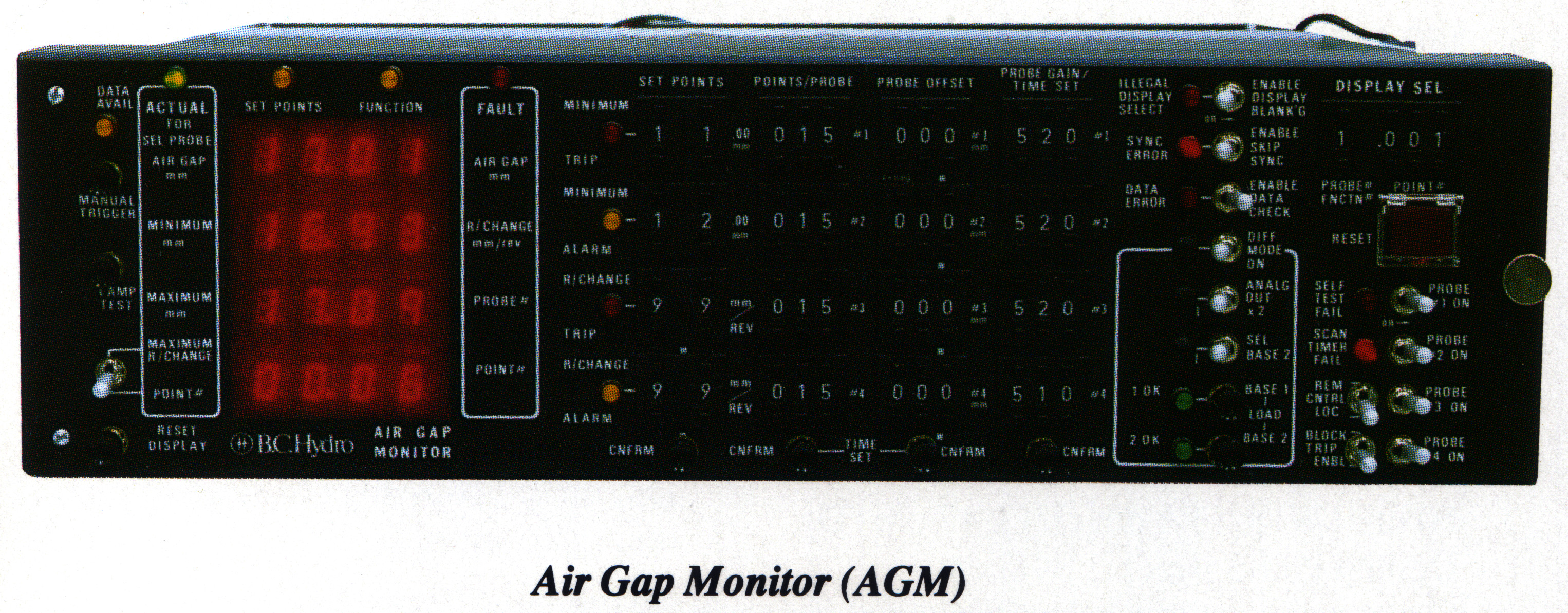
In November 1979, during commissioning at the BC Hydro Peace Canyon Project, a generator suffered significant rotor-stator contact damage. In order to diagnose the cause of this contact, BC Hydro needed dynamic air gap measurements, so they invented and patented (US 4,766,323) a method to measure the air gap between the rotor and stator of a hydroelectric generator while it was running, using retro-reflective optical triangulation. It was developed into their Air Gap Monitor (AGM), as described in this IEEE paper, and could use rotor-mounted as well as stator-mounted sensors.
But the electronics in the AGM that converted the pulses received from the sensors into gap values was rather expensive and had limitations. For example, since the pairs of pulses from each of the two optical paths in a sensor were merged into one signal, at certain gaps they overlapped and were discarded as invalid. A few years later BC Hydro developed their 2nd generation AGM, the Diagnostic Air Gap Monitor (DAGM), that processed the two optical paths separately, so handled overlapped pulses correctly. However, it still had other limitations, and required one large board for each sensor.
In late 1993 I figured out a better method to process the pulses from the air gap sensors, that allowed one small board to handle up to 8 sensors (16 optical paths or channels), rather than needing a separate large board for each sensor or channel. It also increased the range of operation, and had many other improvements. I called it the Digital Timing Module (DTM).
The technique involves a 16-bit counter that increments at the 16 MHz pulse sampling frequency, and whenever any input signal changes its level, a 32-bit record containing the counter value and the current levels of all 16 input signals is written to a FIFO. Since the counter will wrap around to zero many times per second, a record is also written to the FIFO every time the counter wraps. This allows the software on the host computer to extend the counter value to however many bits are needed to eliminate wrapping during one session or in one file, and then to eliminate any records where no input signal changed since the previous record. The FIFO is required because at times the host computer can't process the records as fast as they are being generated, even though it can catch up during quieter periods.
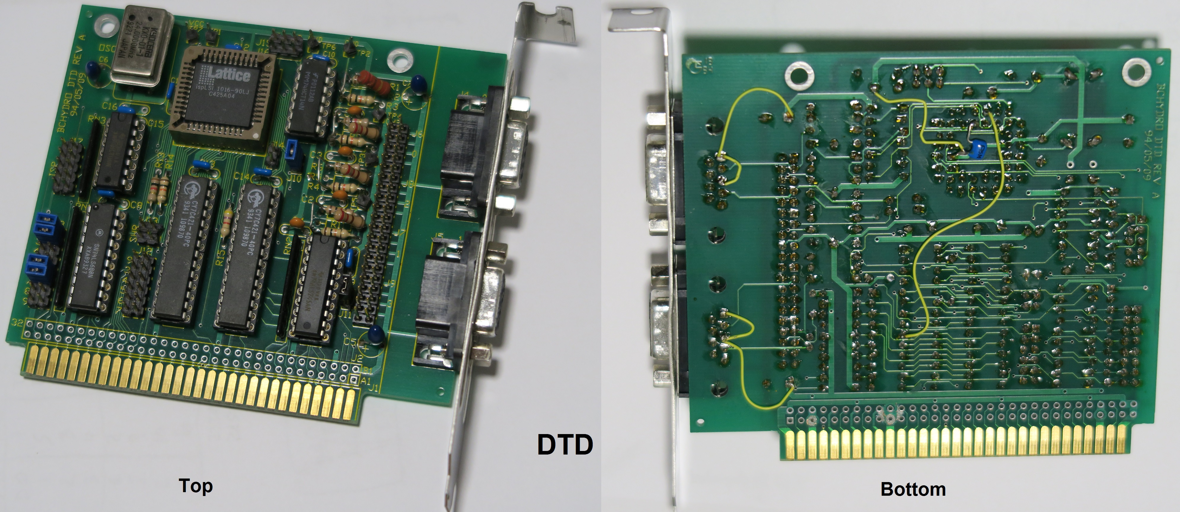
I designed and built a simplified proof-of-concept board (DTD = Digital Timing Demo) with only four input channels, that used the ispLSI 1016 and two Cypress CY7C421 512x9 FIFO chips -- see picture. A former co-worker did the PCB layout for me. The DTD board could be plugged into either an 8-bit ISA bus (IBM PC) connector, or a PC/104 connector. It sampled the pulses at 12 MHz and used a 12-bit counter, generating 16-bit records. One option I tried was using Gray code for the 12-bit count instead of binary.
Several years later I even used this board, with a program written in QuickBASIC, as a simple logic analyzer to debug problems for other clients. The advantage of the DTM/DTD method is that it can capture a short burst of very fast signal transitions, followed by extremely long periods of no transitions, yet generate minimal file sizes.
BC Hydro was interested in using my DTM for their 3rd generation AGM. A brochure was even produced advertising the AB71-AGM3 module for the Allen-Bradley 1771 PLC I/O bus, that incorporated my DTM. But the project was cancelled while still in the concept phase.
According to my notes I also used Lattice CPLDs in other projects for BC Hydro: an ispLSI 1016 in the AB71-IRIGB module that plugged into an Allen-Bradley 1771 PLC chassis, and an ispLSI 1032 in a support board for their Harmonics Filter.
Altera FLEX 10K10
In 1997 I became interested in the Altera FLEX 10K, which seemed to be a hybrid, having features of both CPLDs and FPGAs. It contained CMOS SRAM-based logic elements with 4-input lookup tables (LUT) like an FPGA, but they were grouped into Logic Array Blocks (LAB) like a CPLD. It also had Embedded Array Blocks (EAB) that could implement RAM, ROM, dual-port RAM, or FIFOs, like an FPGA. But instead of segmented routing paths that other FPGAs typically used, the FLEX 10K had lots of long horizontal and vertical routing channels.
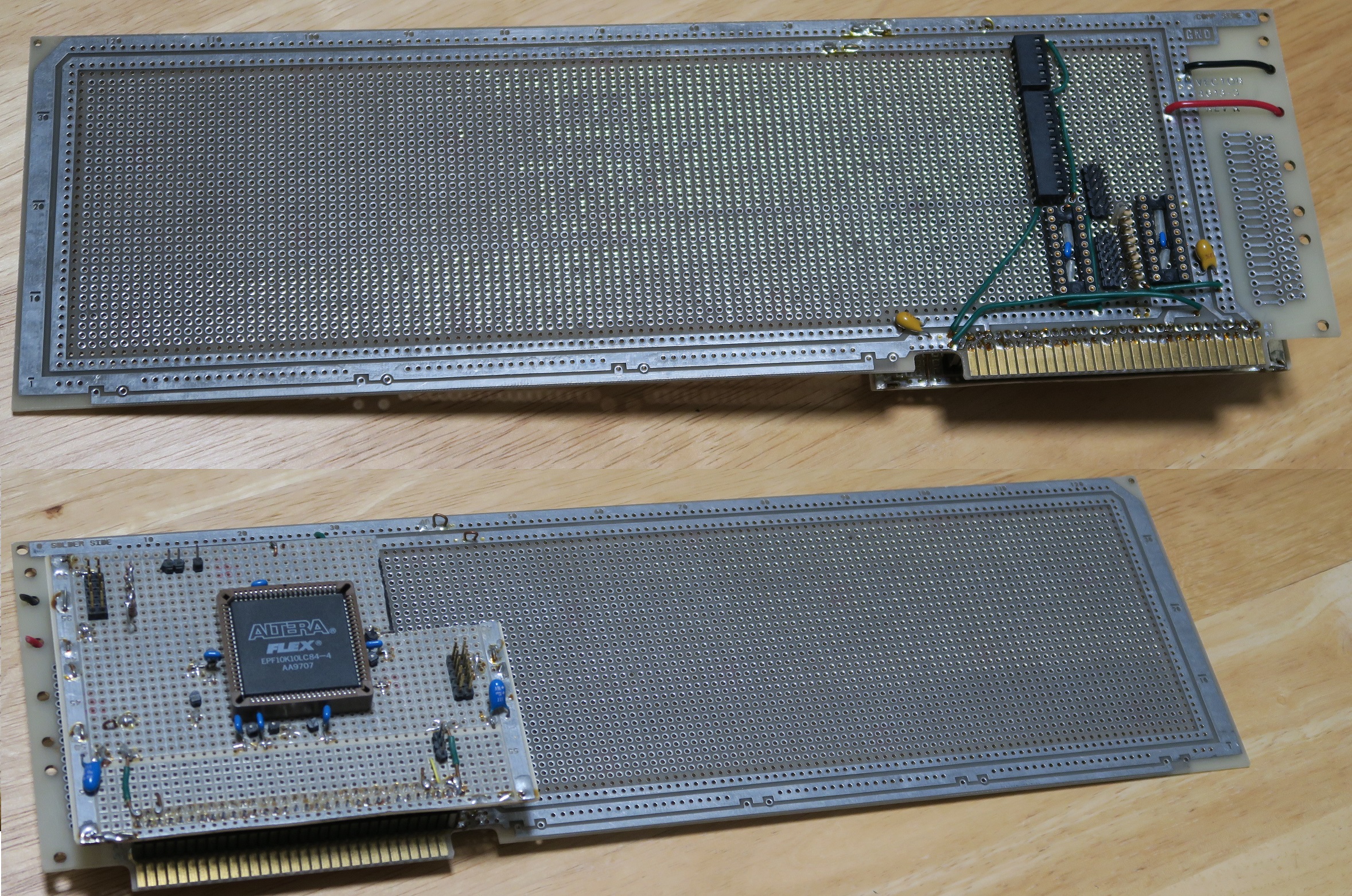
I planned to use the FLEX 10K10 (with 576 logic elements, in a PLCC-84 package) to implement at least two projects. The chip was placed on an 8-bit ISA bus prototyping board -- see picture. But my notes seem to indicate I didn't plug the board into the ISA bus, but kept it outside the PC chassis for easier access, powered from a spare disk drive power cable. Instead of building a clone of the Altera ByteBlaster programmer that plugs into a PC's parallel printer port, my notes say that I connected the parallel port pins directly to the FLEX 10K10 pins, and that I wrote my own software in Turbo C that sent the binary file to the device to configure it.
Both designs used equations written in AHDL (Altera Hardware Description Language), processed with Altera MAX+PLUS II version 6.1 software.
My first FLEX 10K10 project was to be an improved DTD board, that handled many more air gap channels, and used the on-chip EABs as FIFOs, eliminating the expensive external chips. I don't remember finishing this design.

The other project was to try and create a microprocessor core emulating most of the Motorola 6800. I implemented most of the data path, which used approximately half of the logic elements. Could I have fit all the control logic into the remaining resources? Maybe not, but I put the project aside before trying to finish it.
Lattice ispMACH 4064V
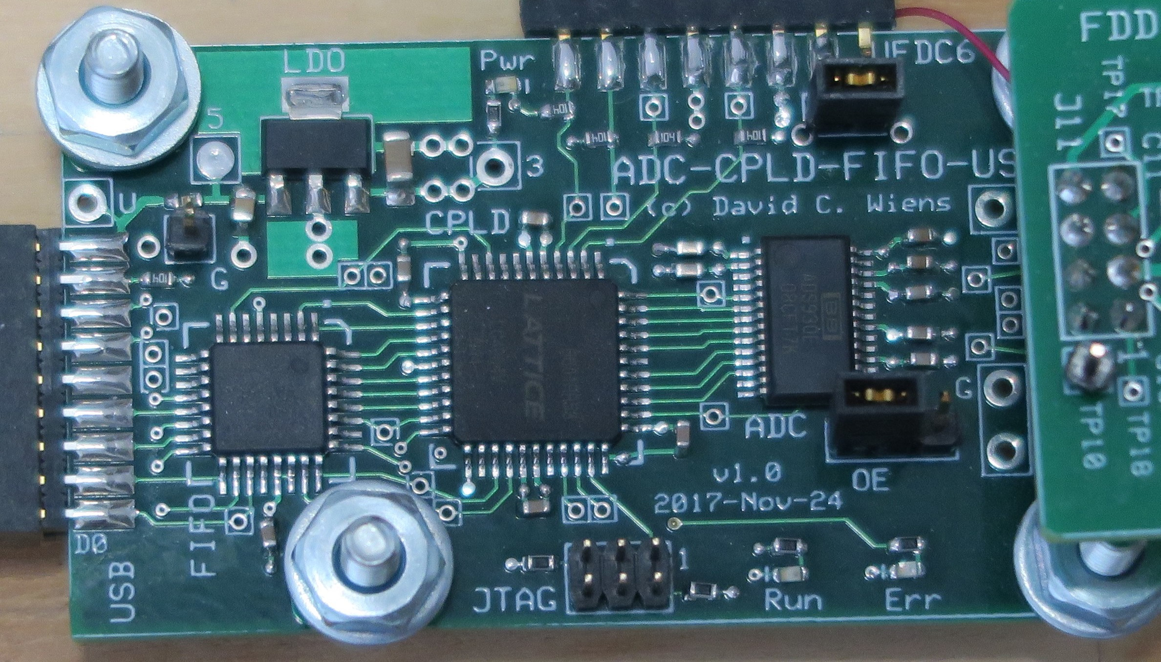
In January 2016 I started designing a device to capture the raw flux signals from a floppy disk drive, in order to image my hundreds of old floppy disks. The final design, which I called the Universal Floppy Disk Reader (UFDR), used a TI ADS930 8-bit pipelined ADC to capture the analog waveform, and a Lattice ispMACH 4064V 44-pin CPLD to capture the digital read signal from the drive, and to merge 8 analog and 8 digital samples (all taken at 15 MS/s) into one 10-byte packet. These packets were written into an IDT 72V241L 4Kx9 synchronous FIFO, which in turn sent them to the host PC via an FTDI FT232H USB-FIFO using its synchronous 245 parallel FIFO mode. The logic equations were written in ABEL and processed with the ispLEVER Classic CPLD design software.
An as-yet-unbuilt project, the ST68F50-ST65F51 ACIA USB-FIFO Module, will use the Lattice ispMACH 4064ZE variant, and be designed with Verilog.
Purchased Boards
Although I didn't design or build these, I have also purchased and used an off-the-shelf Lattice ispMACH 4256V Breakout Board, as well as the WebFPGA ShastaPlus board that uses the Lattice iCE40UP5K FPGA.
Last revised 2026-Apr-15 14:15 PDT.
Copyright 2026- David C. Wiens.
Home Contact Site map